Context: Prime Minister Modi inaugurated SEMICON India on 17 September 2026 in New Delhi which themed ‘Silicon to Systems: Building the Ecosystem.’ It comes two months after the Cabinet approved Semicon 2.0, a ₹1,27,500 crore second phase of India’s chip mission.
What Is a Semiconductor
Semiconductor:
-
- A semiconductor is a material whose electrical conductivity can be precisely controlled. This property allows it to perform functions such as switching, amplification, sensing and signal control.
- The fundamental building block is the transistor which is a microscopic electronic switch.
- Modern integrated circuits can contain millions or even billions of transistors. Hence Semiconductor → Transistor → Integrated Circuit → Electronic System
- They power Artificial Intelligence (AI), telecommunications, electric mobility, defence and advanced manufacturing. Technologies such as the Internet of Things (IoT), 5G/6G, data centres and autonomous vehicles are further driving chip demand.
- Transistor is a microscopic electronic switch. A modern chip packs millions or billions of these onto one small piece of silicon.
How Is a Semiconductor Chip Made?
-
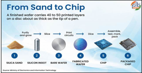
- Silicon is the most widely used semiconductor material. It is obtained from silica, which occurs abundantly in sand. Chip manufacturing begins with highly purified silicon, which is formed into cylindrical ingots.
- These ingots are sliced into thin wafers and polished. Inside fabrication plants, wafers undergo hundreds of carefully controlled processes. These include deposition, photolithography, etching and ion implantation.
- After fabrication, chips go through Assembly, Testing, Marking and Packaging (ATMP), often outsourced as OSAT (Outsourced Semiconductor Assembly and Test). This protects the chip and connects it to other components.
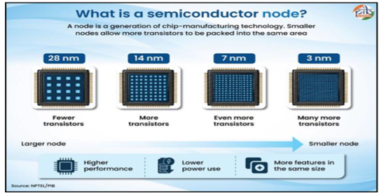
Semiconductor node
A shorthand label (like 28nm or 3nm) for a generation of manufacturing technology. A smaller node can mean higher transistor density and better performance, but real-world performance also depends on design, materials and packaging i.e. node size alone is not the full story.
Why Semiconductors Are a Strategic Resource
-
- Semiconductor Chips power AI, 5G/6G, EVs, defence systems, IoT and data centres. The global semiconductor market grew at 6.5% CAGR (2014-2024) and is projected to grow at 8.5% over the next 5-10 years.
- India spent almost US$150 billion on chip imports during FY17-FY25, growing 23% a year. Demand is projected to hit US$110 billion by FY2030 and cross US$200 billion by FY2035.
- Taiwan alone accounts for over 60% of global chip production and nearly 90% of advanced chips. A level of concentration that worries every major economy, not just India.
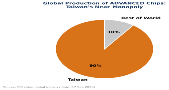
Fig. 1 – Taiwan’s near-monopoly on advanced chip manufacturing is the core global vulnerability India’s policy responds to.
Semiconductors Already Power India’s Strategic Missions
-
- Semiconductor Laboratory (SCL), Mohali: Develops flight-grade, radiation-hardened chips for satellites and launch vehicles.
- Chandrayaan-3: The lander carried an Indian-made camera chip supporting its imaging systems.
- Vikram processor: SCL’s own processor, used in India’s satellite launch vehicles and rockets.
- Aditya-L1: India’s solar mission uses radiation-hardened ADC chips developed by SCL.
From Semicon 1.0 to Semicon 2.0
Semicon 1.0 (December 2021, ₹76,000 crore):
-
- Set up schemes for fabs, display fabs, compound semiconductors and ATMP/OSAT units, plus the Design Linked Incentive (DLI) Scheme.
Semicon 1.0 achievements:
-
- 12 manufacturing units approved (1 silicon fab, 1 silicon carbide fab, 1 GaN Micro LED display fab, 9 ATMP/OSAT units) across Gujarat, Assam, UP, Odisha, Punjab and Andhra Pradesh.
- 5 units already in commercial production.
- 24 chip design projects worth ~₹900 crore & over 1 lakh engineers from 500 organisations (400 academic institutions, 100 startups) given access to chip-design tools.
- 300+ chip designs developed.
Global reach:
-
- Semiconductor cooperation with the US, Japan, EU, Singapore and Netherlands.
- Joint Declaration of Intent with Germany (January 2026) & joined Pax Silica at the AI Impact Summit (February 2026).
- India hosts ~7% of the world’s semiconductor Global Capability Centres and ~20% of the global chip design workforce.
Semicon 2.0 (July 2026, ₹1,27,500 crore):
-
- Government of India approved Semicon 2.0 in July 2026with a total outlay of ₹1,27,500 crore.
- It aims to deepen the capabilities created under Semicon 1.0 and accelerate the growth of a globally competitive semiconductor ecosystem.
- Semicon 2.0 rests on six pillars: design, machines and materials, setting up new fabs, further advanced packaging, research and talent development.
- Its purpose is to buildthe complete chip value chain within the country, and not merely its closing stages. This effort carries India towards supply chain resilience, strategic autonomy and high-value employment in a technology that now underpins every modern industry.
The Supporting Policy Ecosystem
| Scheme | Year | What It Does |
|---|---|---|
| National Policy on Electronics (NPE) | 2019 | Overarching framework for electronics design and manufacturing, including chipsets. |
| SPECS | 2020 | Capital-expenditure-linked incentive for domestic component and semiconductor manufacturing. |
| EMC 2.0 | 2020 | Funds world-class, plug-and-play electronics manufacturing clusters. |
| PLI for Large Scale Electronics | 2020 | Production-linked incentive for mobile phones and components. |
| PLI 2.0 for IT Hardware | 2023 | Boosts domestic manufacturing of laptops, tablets, PCs and servers. |
| Electronics Components Manufacturing Scheme | 2025 | Raised to ₹40,000 crore (Budget 2026-27) to build a component ecosystem and raise domestic value addition. |
| Mobile Phone Manufacturing Scheme | 2026 | Deepens the mobile supply chain and supports Indian brands. |
| Research, Development and Innovation Scheme | 2026 | Funds eligible research projects under Semicon 2.0. |
| 100% FDI in Electronics Manufacturing | Ongoing | Opens the sector fully to global investment and technology partners. |
Comparative View
India’s chip demand is growing fast, but so is its import bill if nothing changes. The real test of Semicon 2.0 is whether domestic fabs can bend that import curve down.
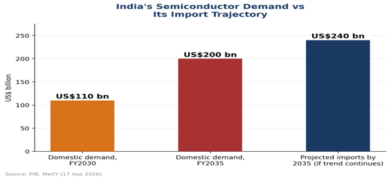
Fig. 2 – Even projected imports by 2035 are close to matching projected demand, if the current trend is not disrupted by domestic manufacturing.
What This Comparison Really Teaches
-
- India is deliberately not chasing the leading edge yet given Taiwan’s near-total dominance of advanced chips. India’s realistic near-term opportunity is the large, less-concentrated mature-node and OSAT market a hedge for global chipmakers wanting options outside Taiwan and China.
- Manufacturing and design capability can grow at different speeds. India can be a genuine design powerhouse while its fabs are still catching up on fabrication nodes.
The Mature-Node Debate
India’s flagship fab i.e. Tata Electronics’ facility at Dholera, Gujarat, built with Taiwan’s PSMC is expected to begin commercial production largely on the 90nm node with capability across 28nm to 110nm. Global leaders like TSMC and Samsung are already at 2-3nm.
-
- The critique: By the time Dholera is fully operational, critics argue that its chips will already be a technology generation or two behind the global cutting edge.
- The counter-argument: Mature-node (28nm and above) chips power automobiles, industrial electronics and IoT devices where global capacity is ‘consistently sold out.’ India does not need to beat TSMC at 2nm to succeed commercially rather it needs a domestic source for the chips that already run the bulk of everyday devices.
- Design is a separate, stronger story: Indian design centres in Bengaluru, Chennai and Hyderabad have done leading-edge design work (including a reported 2nm chip tape-out for a major global chipmaker). Thus, showing India’s strength is currently in design talent, not yet in leading-edge fabrication.
Challenges
-
- The Statesman (September 2026) reported that Tata Electronics’ Dholera fab sits on a taluka with zero freshwater-bearing aquifer area as the site is saline coastal land. So its entire ultrapure water supply must be piped nearly 100 km from the Narmada, a river ‘fully spoken for’ by farms and towns long before the fab was planned.
- It also notes that Gujarat has now committed Narmada water not just to the Dholera fab but also to CG Semi’s Sanand plant and Micron’s packaging unit (over 20 million litres a day, scalable to 90 million).
- ORF notes that high sunk costs and R&D expenditure make the industry difficult to scale even for advanced economies
- India still depends entirely on foreign toolmakers like ASML, Applied Materials and Lam Research for fab equipment.
- ORF highlights gaps in research output and patenting as constraints on India’s transition from design strength to a broader innovation base.
Way Forward
-
- MeitY and NPCIL/DAE should accelerate round-the-clock power sourcing (including the SHANTI Act’s nuclear push) for fabs and OSAT units.
- The Ministry of Electronics and IT should continue backing mature-node and OSAT capacity as the near-term priority, while using the Research, Development and Innovation Scheme to build a credible pathway toward advanced nodes over the next decade rather than promising both at once.
- Financial incentives should increasingly be linked with measurable outcomes such as domestic value addition, technology transfer, R&D, yield improvement and supplier development, rather than focusing only on plant establishment.
- Industry and government together should keep building the ‘machines and materials’ pillar domestic equipment and materials manufacturing as the genuine long-term fix for import dependence.
- Since India’s ~20% share of the global chip design workforce and recent leading-edge design wins (like the reported 2nm tape-out) are its most globally competitive asset today, ahead of fabrication.
Conclusion
Nevertheless, India’s semiconductor journey has moved from zero commercial chip plants in 2021 to twelve approved units and five in production by 2026. If India can successfully combine its large market, chip-design capabilities and international partnerships with R&D capabilities. Then, semiconductors can become an important pillar of technological self-reliance, and high-value industrialisation.
Spread the Word